Page 1 of 1

Centaur Technologies Tour - Making The Via Nano CPU

Posted: Mon Jun 02, 2008 7:00 pm
by Apoptosis
Centaur Technologies Tour - Making The Via Nano CPU

Last week VIA Technologies announced the new VIA Nano processor family based on the VIA Isaiah Architecture. Legit Reviews was visiting Centaur Technology, the company behind the VIA Nano. The crew over at Centaur gave us a tour and showed us how they make low-cost x86 compatible microprocessors. We also talk about the VIA Nano and show off some benchmark numbers. The Intel Atom better watch out!

Image
Pictured above are eight full trays of VIA Nano processors that are ready to be sorted! They had thousands of freshly cut and made Nano processors that were ready for testing if you looked around the room. It should be noted that the entire VIA Nano processor family uses Fujitsu's 65 nanometer process technology for and features a compact 21mm x 21mm nanoBGA2 package. Once Centaur gets the wafer back from Fujitsu they then complete the assembly of the processor and move on to testing and speed binning.
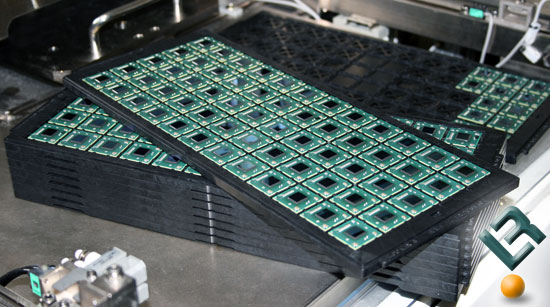
Article Title: Centaur Technologies Tour - Making The Via Nano CPU
Article URL: http://www.legitreviews.com/article/719/1/

Re: Centaur Technologies Tour - Making The Via Nano CPU

Posted: Mon Jun 02, 2008 7:19 pm
by dicecca112
Woohoo Fixing Via Nano for Ubuntu!

Re: Centaur Technologies Tour - Making The Via Nano CPU

Posted: Mon Jun 02, 2008 7:33 pm
by DMB2000uk
This is much better than just a launch day tech article about the Nano. :mrgreen:
(but those are still good when that's all you can do!)

Thanks Nate!

Dan

Re: Centaur Technologies Tour - Making The Via Nano CPU

Posted: Wed Jun 04, 2008 9:36 pm
by mhwong
Interesting review - a pity that you don't get to see a picture of a Nano wafer but I suppose they really wants to keep the information away from the competitor for now (layout, density, etc) - but we have a saying in the industry that there is no secret in semiconductors.

WD40 is a rather common - in the assembly lines where I work we buy them by the cartons. And that tape next to it seems like a roll of Kapton(tm) tape - rather high temperature capable tape for assembly use.

Re: Centaur Technologies Tour - Making The Via Nano CPU

Posted: Thu Jun 05, 2008 5:03 am
by Apoptosis
mhwong wrote:Interesting review - a pity that you don't get to see a picture of a Nano wafer but I suppose they really wants to keep the information away from the competitor for now (layout, density, etc) - but we have a saying in the industry that there is no secret in semiconductors.

WD40 is a rather common - in the assembly lines where I work we buy them by the cartons. And that tape next to it seems like a roll of Kapton(tm) tape - rather high temperature capable tape for assembly use.
Thanks for joining the forums and sharing your inside knowledge! You guys always fill in the blanks and make it fun!

Re: Centaur Technologies Tour - Making The Via Nano CPU

Posted: Thu Jun 05, 2008 8:33 am
by KnightRid
So what was the fix for the ubuntu problem, or would you have to be killed if you told us ? :)

Factory tours are the best! Especially if they hand out freebies :mrgreen:

Mike

I would be curious to see how the cpus stand up to video decoding, say for a HTPC that is TINY! Maybe a dual or quad setup? Depends on pricing whether it would be cost effective or not though.

Re: Centaur Technologies Tour - Making The Via Nano CPU

Posted: Thu Jun 05, 2008 8:40 am
by Apoptosis
KnightRid wrote:So what was the fix for the ubuntu problem, or would you have to be killed if you told us ? :)

Factory tours are the best! Especially if they hand out freebies :mrgreen:

Mike

I would be curious to see how the cpus stand up to video decoding, say for a HTPC that is TINY! Maybe a dual or quad setup? Depends on pricing whether it would be cost effective or not though.
They just had to blow a different fuse than the one that was previously blown, so the fix was quick and simple. As for freebies... None on this trip, not even a pen!